
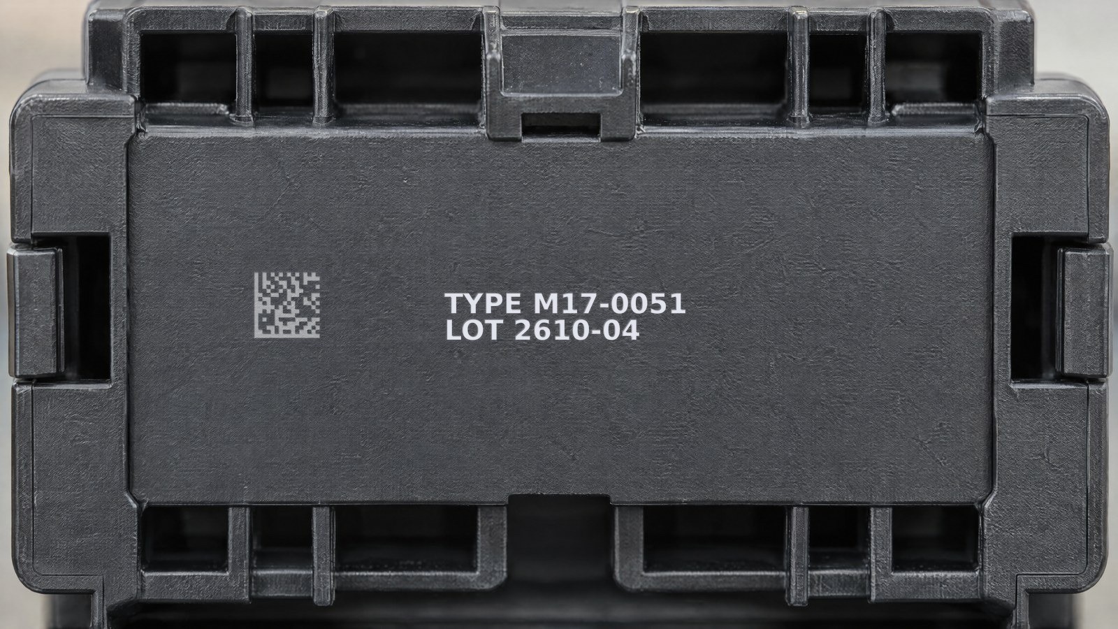
Those who industrialize marking in electronics work on a tight margin. Thin plastic packages, connectors with contacts a few hundredths of an inch apart, encapsulation resins, modules already populated with solder joints and traces: these are surfaces onto which you have to imprint serial numbers, DataMatrix codes and lot references, but where any excess energy risks degrading what lies beneath or beside the marked spot.
The worst defect, in this context, is the one you can’t see during a visual inspection. A resin that chars at the edge, a microcrack induced by thermal stress near a joint, an electrostatic discharge picked up during handling: these are causes of returns that show up in the field, not on the inspection bench. The process question isn’t how much energy it takes to mark, but how little of it is left around the spot that was struck.
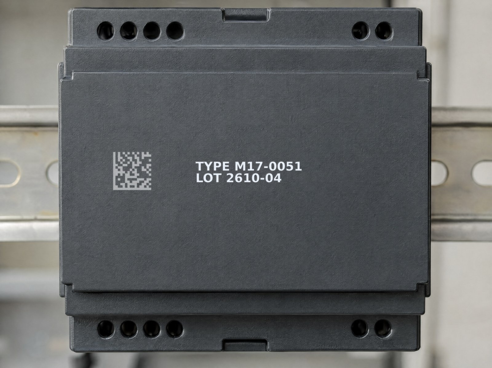
This is where the picosecond pulse changes the game: it transfers energy over such short time spans that the heat input to the surrounding material becomes negligible, and it does so as a non-contact process, with no mechanical pressure on the component.
Cold ablation: why the thermal impact stays negligible
Traditional fiber marking, with pulses on the order of nanoseconds, works largely through a thermal mechanism: the material is heated, melted and partly oxidized. Around the marked spot a heat-affected zone (HAZ) forms, in which the heat has spread before dissipating. On a solid metal it’s irrelevant; on a plastic package a few hundredths of an inch thick or on a resin encapsulating a chip, that diffusion is exactly what you can’t afford.
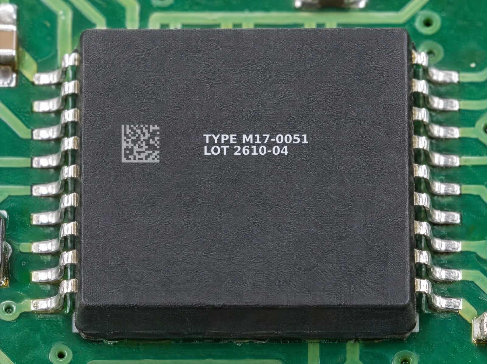
The picosecond pulse flips the relationship between the energy-release time and the heat-diffusion time. The pulse duration is on the order of 10⁻¹² seconds, shorter than the time heat takes to propagate through the material’s lattice. The energy removes the surface layer by ablation before turning into heat that would warm the surroundings: this is why it’s called “cold” ablation. The thermal impact isn’t eliminated — a residual share always exists — but it stays negligible, and the HAZ shrinks to a fraction of that of a long pulse. It’s no coincidence that the picosecond laser is the established choice wherever you need to mark without reflection and without altering the substrate.
Pulse duration Heat-affected zone shorter pulse, smaller HAZFor the process engineer this translates into a much wider working margin: you obtain a clean, legible mark while keeping the substrate well below the thresholds at which plastics and resins start to soften, blister or char.
Packages, connectors and resins: marking without attacking the substrate
Electronics materials are unforgiving. The epoxy compounds of packages, the technical thermoplastics of connectors and the encapsulation resins have low thermal thresholds and behave differently from one another: some blister, some discolor uncontrollably, some deform. With a long pulse the trade-off is constant: lowering the energy to avoid damage often means a weak mark, raising it to make the mark legible means risking the substrate.
The ultrashort pulse dissolves this trade-off because it acts on the outermost layer. On packages it modifies the first few microns of the material in a controlled way, generating contrast without digging deep and without affecting the component’s functionality. On connectors and resins the mark stays confined to the intended area, without propagating stress to the body of the part. It’s the same logic that governs marking plastics in the electronics sector, where the compatibility between source and material determines the quality of the result.
Distance from joints and traces: the marking layout matters
On an already populated module the mark doesn’t live on its own: it coexists with solder joints, bumps, leads and traces that must not receive energy. The advantage of the picosecond here is twofold. The beam is tightly focused, so the energy stays concentrated in a narrow area; and the negligible lateral heat diffusion ensures that what happens at the marked spot doesn’t “spill over” toward the nearby conductors.
There remains, however, a rule of good design: define a dedicated marking area on the package, with a safety margin from the leads and traces, and validate it during trials on real samples. It’s a layout task you do once, up front, and it makes the cycle repeatable in production. The FlyCAD software handles the placement of the content — serial numbers, DataMatrix, logos — within the assigned area, so the mark always lands where it should.
Non-contact process and in-line ESD management
Sensitivity to electrostatic discharge is a matter of handling, not just of marking. Compared with methods that touch the part — punching, dot peen, pad printing with contact — laser marking is a non-contact process: no tool presses on the component, no friction generates charges at the work point, and there’s no mechanical wear introducing conductive particulate.
This doesn’t exempt you from the line’s good ESD practices: the component still has to be handled in a controlled environment, with grounded equipment and work surfaces and proper management of nests and part-carrying pallets. Non-contact marking eliminates one of the sources of stress — the mechanical and electrostatic one from direct contact — and integrates into automated stations where the part stays in its antistatic fixture throughout the cycle.
Contrast and legibility on matte black
Most electronic packages are a matte black: precisely the color on which it’s hardest to achieve a legible, stable code. With the picosecond pulse the contrast comes from a controlled surface modification, which produces a clear, crisp and non-iridescent mark: the code keeps the same contrast from any viewing angle, an essential condition for automatic in-line reading of DataMatrix codes.
Contrast stability is what distinguishes a mark that passes inspection from one that generates false rejects. A DataMatrix on a black package has to stay legible after handling and downstream processing; cold marking, based neither on surface oxidation nor on a deep engraving, offers constant contrast over time. Formal verification of code quality requires controlled laboratory conditions, while in-line grading remains the practical tool for keeping legibility under control during production.
When UV makes more sense than picosecond
Picosecond isn’t the answer to every marking job in electronics, and it’s only fair to say so. Its strength is versatility on mixed substrates — metal, packages, resins, dark surfaces — with negligible thermal impact. But when the part is a light-colored or transparent plastic, or a polymer that’s particularly reactive to short wavelengths, the UV laser at 355 nm works through a predominantly photochemical absorption and often generates better contrast with even less energy in play: this is the domain of the UV laser for plastics.
| Criterion | Picosecond fiber (1064 nm) | UV (355 nm) |
|---|---|---|
| Predominant mechanism | Ultrashort-pulse ablation, negligible heat input | Photochemical absorption, low energy in play |
| Ideal materials | Mixed metal-plastic substrates, packages and resins, dark surfaces | Light-colored and transparent plastics, thin films, sensitive polymers |
| Contrast on matte black | High and non-iridescent, stable over time | Good on many plastics, variable on heavily pigmented blacks |
| In-line strength | A single source for heterogeneous product families | Maximum gentleness on light-colored polymers |
The choice, in practice, is made based on the material and the required result, not on principle. On dark packages and connectors, on mixed substrates and where a single source is needed for heterogeneous product families, the picosecond is the most rational solution. On light-colored plastics, thin films and components where even the slightest heat input must be avoided, it’s worth evaluating UV. On many lines the two technologies coexist, each on the job it does best.
In short: if you mark sensitive electronic components — black packages, connectors, populated modules — and the problem is obtaining legible codes without thermal damage and without contact stress, the picosecond fiber tackles exactly that. The validation has to be done on your own materials, with trials on real samples: that’s where the process margin is truly measured.

Applications Manager | LASIT
Applications Manager at LASIT for over 20 years, Mario Palmieri oversees the management and development of the company’s laser laboratory. He is responsible for conducting sample tests for customers, supporting the automotive, medical, aerospace and electronics sectors in identifying the most suitable laser marking solution for their needs.


